
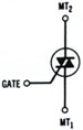
The triac is a three terminal semiconductor for controlling current in either direction. Below is the schematic symbol for the triac. Notice the symbol looks like two SCRs in parallel (opposite direction) with one trigger or gate terminal. The main or power terminals are designated as MT1 and MT2. (See the schematic representation below) When the voltage on the MT2 is positive with regard to MT1 and a positive gate voltage is applied, the left SCR conducts. When the voltage is reversed and a negative voltage is applied to the gate, the right SCR conducts. Minimum holding current, Ih, must be maintained in order to keep a triac conducting.
A triac operates in the same way as the SCR however it operates in both a forward and reverse direction. To get a quick understanding of its operation refer to its characteristic curve below and compare this to the SCR characteristic curve. It can be triggered into conduction by either a PLUS (+) or MINUS (-) gate signal.
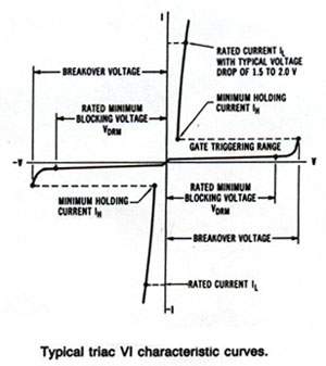
Obviously a triac can also be triggered by exceeding the breakover voltage. This is not normally employed in triac operation. The breakover voltage is usually considered a design limitation. One other major limitation, as with the SCR, is dV/dt, which is the rate of rise of voltage with respect to time. A triac can be switched into conduction by a large dV/dt. Typical applications are in phase control, inverter design, AC switching, relay replacement, etc.
Major considerations when specifying a triac are:
(a) Forward and reverse breakover voltage.
(b)Maximum current
(c) Minimum holding current
(d) Gate voltage and gate current trigger requirements.
(e) Switching speed
(f) Maximum dV/dt
Leave A Comment