
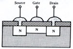
A FET with an oxide coating between gate and channel is called a MOSFET (metal- oxide semiconductor field effect transistor). The figure below shows the oxide, insulating the gate from the channel. As a result, the MOSFET has very high input resistance, higher than the JFET; and as with the JFET, the gate controls the main or channel current, Ids.
Notice that a positive gate voltage will induce a negative charge in the n-channel, enhancing the drain-source current, Ids; while a negative gate voltage will induce a depletion region in the n- channel, thereby reducing the drain-source current, Ids. A MOSFET so constructed is a depletion/enhancement MOSFET. A typical n-channel MOSFET curve is shown below:
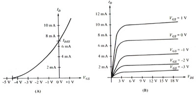
Figure (A), shows the transconductance, Gm, or effect of the gate voltage upon the drain to source current. Notice the gate-source voltage can be positive or negative. This would not be possible with a JFET. In figure (B), again notice the effect of increasing Vgs on Ids; notice also that for any given gate current, the drain-source voltage has little effect upon the drain current above 3 volts, since the MOSFET is in saturation.
The MOSFET is also made in an enhancement-only mode, where a gate signal only induces or enhances channel current, the gate signal never depletes the channel current. Naturally there are p-channel enhancement MOSFETS, where a negative gate voltage enhances channel conductivity; and n-channel enhancement mode MOSFETS where a positive gate voltage enhances channel conductivity. One final note, breakdown voltage in MOS devices do not depend upon p-n junction stress but rather upon the thickness and quality of the insulating oxide. When breakdown does occur, the oxide is punctured and the device is destroyed. The specifications for MOSFETS or any transistor are multitudinous, and so only the basics are listed. They are:
(a) Breakdown Voltages
(b) Forward transconductance
(c) Drain- source on resistance , Rds(on)
(d) Switching characteristics
(e) Zero gate voltage drain current, Idss
(f) Input capacitance, Ciss
Leave A Comment