
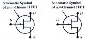
The J-FET (Junction Field Effect Transistor ) and the MOS-FET (Metal-Oxide-Semiconductor FET) are voltage controlled devices: that is a small change in input voltage causes a large change in output current. FET operation involves an electric field which controls the flow of a charge (current) through the device. In contrast, a bipolar transistor employs a small input current to control a large output current. The source, drain, and gate terminal of the FET are analogous to the emitter, collector, and base of a bipolar transistor. The terms n-channel and p- channel refer to the material which the drain and source are connected. Below is the schematic symbol for the p-channel and n-channel JFET:
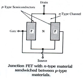
A simplified n-channel JFET construction is shown below. Note that the drain and source connections are made to the n-channel and the gate is connected to the p material. The n material provides a current path from the drain to the source. A n-channel JFET is biased so that the drain is positive in reference to the source. On the other hand, a p-channel JFET with n material gate would be biased in reverse.
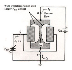
As with any reversed biased PN junction, a depletion region is formed which increases as the reverse gate voltage is increased. This depletion region, being devoid of majority carriers, reduces the channel drain-source current. See figure below:
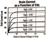
As a result, the the drain-source current is controlled by the gate voltage. Referring to the figure below, a typical JFET characteristic curve; notice the effect of the gate-source voltage on the drain-source current, Ids. Notice the near linear relationship of drain current to drain voltage from zero to about one volt after that the JFET saturates. However, as the gate voltage is increased, the drain-source current is increased.
The figure of merit, Gfs, that is the ratio of drain-source current to gate voltage is the JFET transconductance. As with the bipolar transistor, there can be many relevant specifications, depending upon the JFET circuit application, however the most common parameters are:
(a) Gate source breakdown voltage, BVgss
(b) Gate reverse leakage current , Igss
(c) Gate source cutoff voltage , Vgs(off)
(d) Drain current at zero gate voltage , Idss
(e) Forward transconductance, Gfs
(f) Input capacitance, Ciss
(g) Switching considerations
(h) Drain-source on resistance, Rds(on)
Leave A Comment