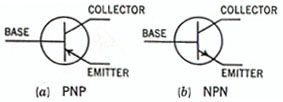
Bipolar transistors, having 2 junctions, are 3 terminal semiconductor devices. The three terminals are emitter, collector, and base. A transistor can be either NPN or PNP. See the schematic representations below:

Note that the direction of the emitter arrow defines the type transistor. Biasing and power supply polarity are positive for NPN and negative for PNP transistors. The transistor is primarily used as an current amplifier. When a small current signal is applied to the base terminal, it is amplified in the collector circuit. This current amplification is referred to as HFE or beta and equals Ic/Ib.
As with all semiconductors, breakdown voltage is a design limitation. There are breakdown voltages that must be taken into account for each combination of terminals .i.e. Vce, Vbe, and Vcb. However, Vce (collector-emitter voltage) with open base, designated as Vceo, is usually of most concern and defines the maximum circuit voltage.
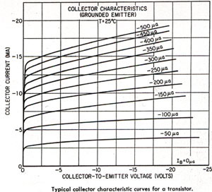
Also as with all semiconductors there are undesirable leakage currents, notably Icbo, collector junction leakage; and Iebo, emitter junction leakage. A typical collector characteristic curve is shown below:

Note that the negative collector-emitter voltage tells you that the transistor is PNP. Also that the output current increases with input or base current and varies very little with collector-emitter voltage.
Primary considerations when selecting a transistor are:
(a) Voltage ratings of all three junctions
(b) Power rating and thermal resistance
(c) Current handling capability and the transistor case size
(d) Leakage currents, mainly Icbo and Iebo
(e) Frequency response and /or switching times.
(f) Current gain (HFE and hfe)
(g) Temperature parameter variation.
(h) Saturation resistance
(I) h-parameters for linear applications


Leave A Comment